
Determine VCE and Ic
When you start to learn how to use ADS, the first project might be designing an amplifier. In this blog, I will show you how to design an amplifier using BFP650, step by step. Assuming that it will work at 2GHz.
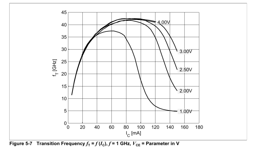
First things first, let’s take a look at BFP650’s datasheet. Figure 1 shows the variation of transition frequency with collector current. It shows that the transition frequency reaches maximum at Ic=80mA and Vce at 3V-4V.
Then let’s start simulation!
Install Design Kit
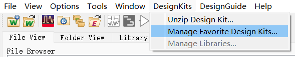
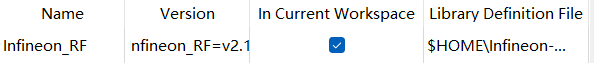
You can get the Infineon RF Transistor design kit here. Unzip this compressed file, open ADS and add the design kit you just downloaded.
Now we can add Infineon RF transistor in schematics now.
DC Simulation
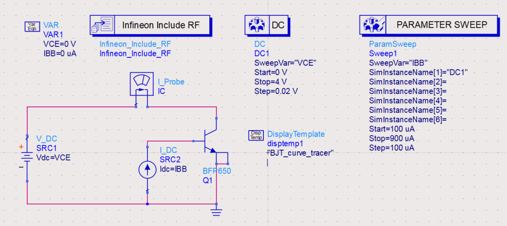
DC simulation matters because it helps us determine the operating point. All other simulations are based on DC simulation. Make sure you rename the instance name of IC_probe to IC. Then add a display template of “BJT_curve_tracer” into the schematic, which is presented in figure 4.
After running the DC simulation, we will see the data display page. Figure 5 shows how IC varies with VCE in different values of base current(IBB).
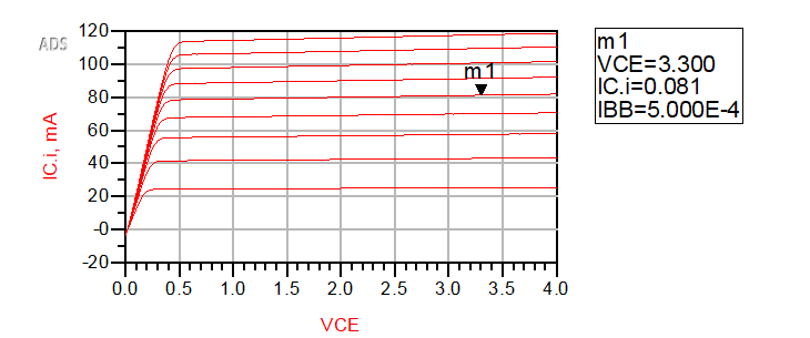
To amplify, BJT must work in saturation region. It seems m1 is a good operating point, with VCE=3.3V and IC=81mA. So it consumes 268mW, while from datasheet, we know that it can stand 500mW at room temperature(25℃). It may seem this power consumption is a little too much, especially when VCE drops to 2V, the transition frequency does not drop much.(See figure 1) But for now, let’s set it aside.
Design Bias Network
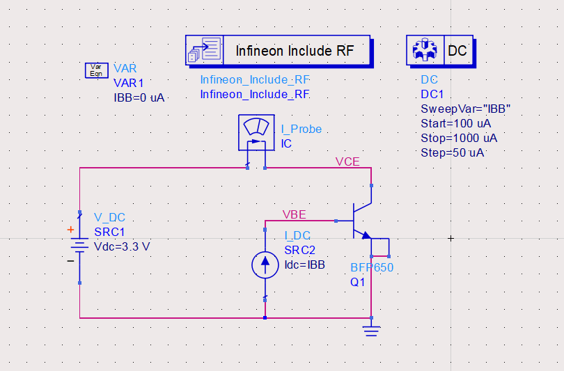
Nobody is willing to use a current source to drive the base of such a little BJT, for which we will design a bias network, making the BJT work at the desired operating point. We will use two lumped resistor to design the bias network. And figure 6 is the schematic how we can get the value of them.
Assuming Vcc=5V, we can get two equations.

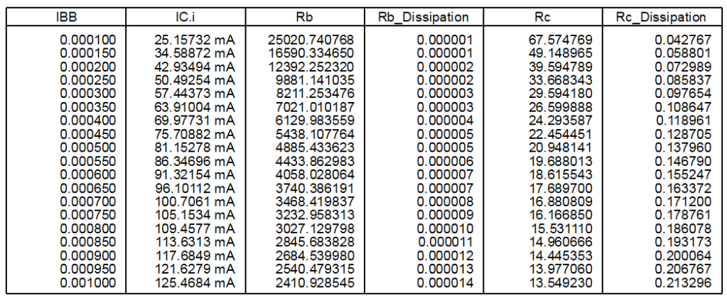
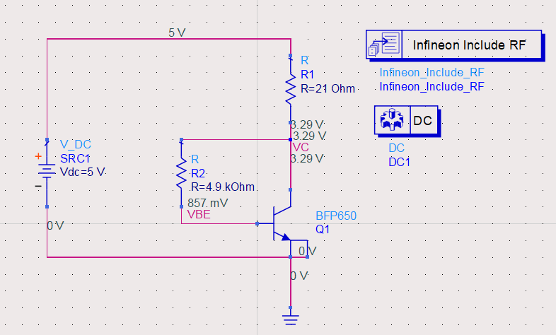
We want Ic to be about 80mA, so IBB=500uA, Rb=4.9kΩ, Rc=21Ω. Now we create a new schematic and see whether DC voltage of each node is correct. The schematic is shown in figure 8. And from annotations its operating point is as expected. Besides, by sweeping parameter temp, we can see how temperature affects VCE and VBE.
AC Simulation
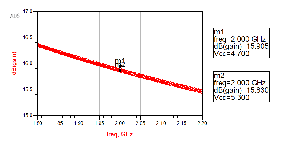
As operating point is determined, it’s time to see how much the gain at 2GHz is. With the schematic in figure 9, we can do a basic AC simulation to see it.
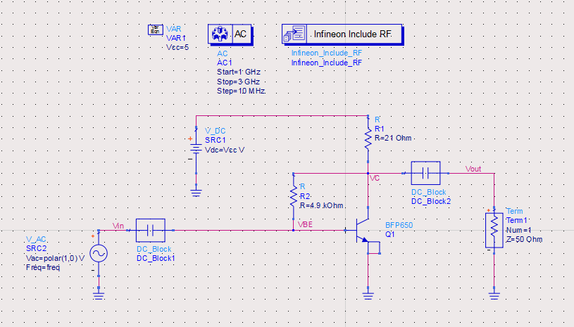
Then we set AC small-signal simulation controller ,open noise tab, enable noise calculation, add node “Vout”, and sort noise contributors by value. At last run the simulations. In the data display page, we add two equations, 

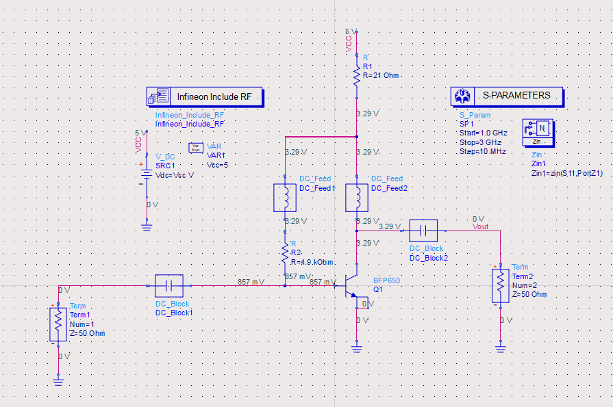
S-Parameter Simulation
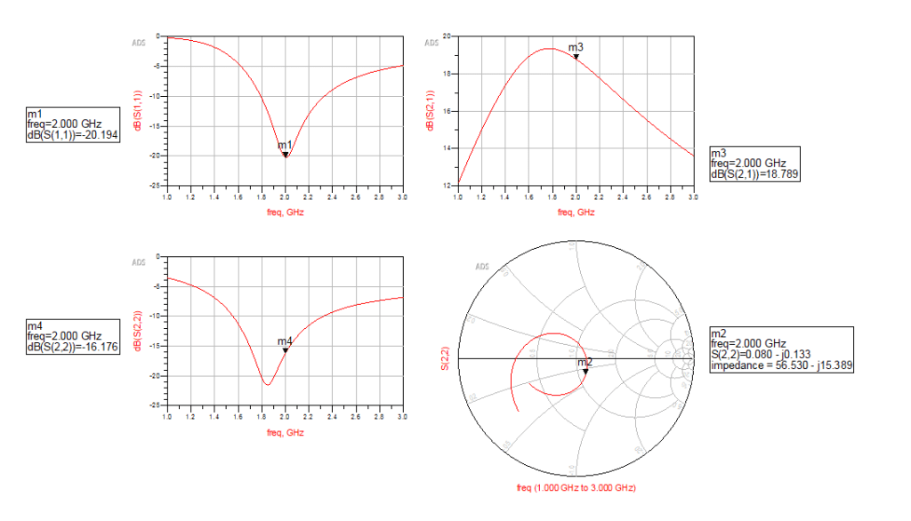
To optimize performance of the amplifier, we must do impedance matching, and S-Parameter Simulation can help. The schematic is shown in figure 11.
From S11, we know that 
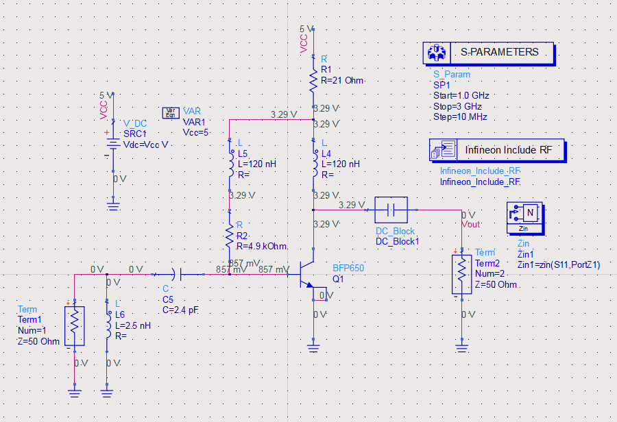
In data display page, we can see that S11 at 2GHz is very small(around -32.7dB) but S22 is -13dB(It is ok, but we can do it better). From S22 Smith chart, we know 
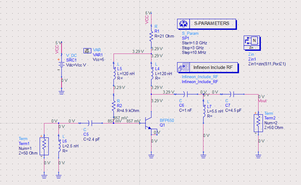
Then we found S11 increase to -13.5dB, which means we should optimize the match network at port 2 to decrease S11. Then we enable the tuning options of C7 and L7 ,then tune their values. Generally, we want both S11 and S22 less than 15dB. It’s easy to achieve in this example.
Harmonic Balance Simulation
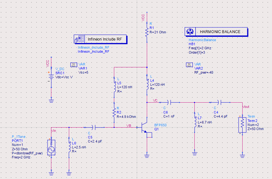
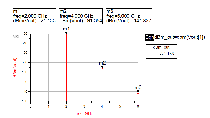
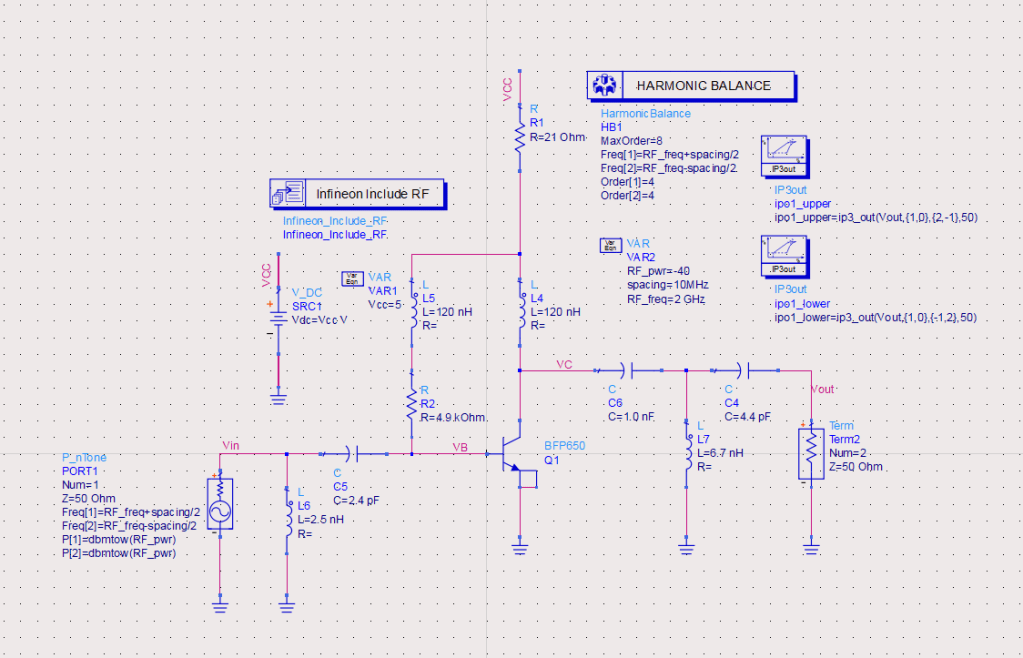
Harmonic balance simulation is a frequency-domain analysis method to simulate non-linear systems. It can help us evaluate non-linearity of a system. For an amplifier, harmonic balance simulation can give general AC characteristics such as IPO3 and P1dB. In this example, we will see how harmonic balance simulation work. Figure 14 is the schematic of the one tone harmonic balance simulation and figure 15 shows the non-linearity.
In practice, input signal is not single tone, so we need to use multiple tones harmonic balance simulation. Assuming the bandwidth is 10MHz, let’s see the non-linearity characteristics. We add a P_nTone source, and set the schematic as the figure 16 below. By adding two IP3out calculation part, we can get IP3 at the data display page. The output IP3 is about 36dBm.
Circuit Envelop Simulation
Circuit Envelop Simulation simulates high-frequency amplifiers, mixers, oscillators, and subsystems that involve transient or modulated RF signals. It is highly efficient in analyzing circuits with digitally modulated signals, because transient simulation takes place only around the carrier and its harmonics. In addition, its calculation are not made where the spectrum is empty(assuming most of the frequency spectrum is empty).
To run circuit envelop simulation for this amplifier, we add a GSM source and a circuit envelop simulation controller, then configure them as below.
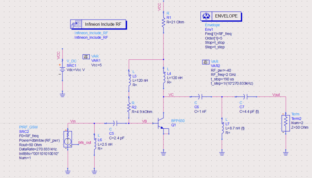
Run and open data display page, then add a equation![baseband=diff\left( unwrap\left( phase\left( Vout\left[ 1 \right] \right) \right) /360 \right)](https://s0.wp.com/latex.php?latex=baseband%3Ddiff%5Cleft%28+unwrap%5Cleft%28+phase%5Cleft%28+Vout%5Cleft%5B+1+%5Cright%5D+%5Cright%29+%5Cright%29+%2F360+%5Cright%29&bg=ffffff&fg=000&s=0&c=20201002)

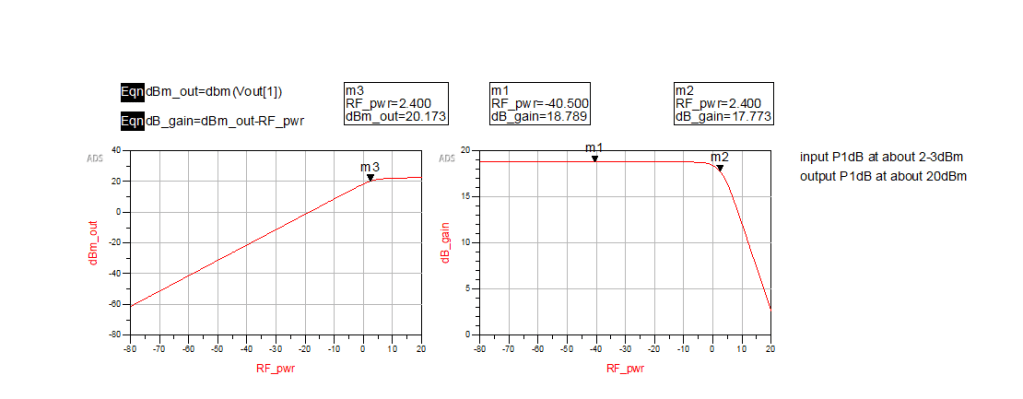
Gain Compression Simulation
Gain compression simulation is a large signal simulation. We can get P1dB by running this kind of simulation. The P1dB of this amplifier is 20dBm. Besides, harmonic balance simulation can also help us get P1dB, by sweeping the power of input signal and calculate the gain of fundamental wave, just as figure 19 presents.
One response to “To make an amplifier from a BJT”
-
By the way, all the simulation files are uploaded to https://github.com/liwuguibo/ADS-Learn-Note/tree/main/Others/AMP_BFP650
LikeLike

Leave a comment